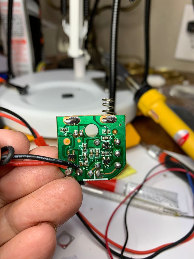
About: Hi! I am Angelo, others know me as TechBuilder. I am an Electronics & Communications Engineering main. Instructables has been my house ever since I was 10. Hope yall get pleasure from my initiatives! Today I’m going to show you tips on how to make your very personal custom-made PCB (printed circuit board). All you need are some supplies and instruments like a: PCB board, A bottle of Ferric Chloride, A mini drill, A small container, A bottle of thinner and a few plastic tweezers. Making your personal circuit board solely takes a snap, what you need is 30-45 minutes of time. It is so easy even a 12 year old child could make one ! What are PCBs ? PCB (printed circuit board (git.sicom.gov.co)) is used to mechanically help and printed circuit board electrically join electronic elements utilizing conductive pathways, tracks or signal traces etched from copper sheets laminated onto a non-conductive board. Components are connected by way of the conductive material below a non conductive board, the common conductive material utilized in packaged PCBs are normally copper, since copper is cheap and common. Why Use Customized PCBs Instead of Ready Made Project Board? First, PCB as a result of the board shall be extra compact because your design as properly is made to be compact. Second, it’s extra handy to make use of, since you possibly can determine where to place area in your board. And last, the board will be stronger unlike these prepared made project boards are filled with holes everywhere, making ready made boards weaker. How Can we Make Them ? Usually you print your circuit design not directly to your board, you print it on a glossy paper, photo paper or journal paper. Let me remind you that before you print it is best to use a laser printer or a photocopying machine, utilizing of inkjet printer is not going to work. After you had printed your circuit board design you’ll iron the printed design over the copper facet of the PCB, ironing it above the copper aspect of the board will transfer the ink, from the glossy paper to the PCB board. The ink serves as the protecting layer to cowl the copper half that shouldn’t be etched. Then after transferring the ink to the PCB board you’ll have to dip the PCB board to a etching solution like Ferric Chloride for 15 minutes. After etching it you might must rinse the PCB board with water to take away the etching answer. After rinsing it it’s best to take away the remaining ink with thinner, Pcb Board Buying Guide to uncover the uneched copper part. After eradicating the ink you will need to dill holes on your parts to be soldered on the board. And final however not least just solder your elements of your personalized board and printed circuit board your finished! How does the process work? The video below is just not mine! Its the courtesy of javapda. The Peel n Press paper point out may be substituted with a journal paper or photograph paper.